The official site of 9Club online casino has a short history of existence but deserves a fairly high rating due to the presence of a confirmed license, good bonuses and some other advantages. Even a small collection of gambling entertainment does not diminish the interest of players in this project.
About online casino
9Club online casino was launched only in 2017. The creators of the project received a license from the Curacao gambling regulator, but the site does not say anything about it. You can find out about the availability of official permission only from the technical support service.
All information on the site is available exclusively in English, since the main target audience of the operator was originally players from Asia. In the footer, the operator has placed links to pages with Terms and Conditions, FAQ, company information, contact information, and so on. At the right edge of the screen, you can see a small green button with a vertical Feedback. Clicking on it opens a small window, it offers to evaluate the quality of the casino and leave a review or suggestion that the administration will see.
Bonuses and promo codes
Welcome Bonus. It consists of five cash bonuses that are awarded for the first deposits. In total, the operator gives players up to 0,13 BTC. Bonus money is not allowed to play at tables with live dealers. Wager x30 applies not only to the funds donated by the operator, but also to the amount of the deposit. 30 days are given for wagering.
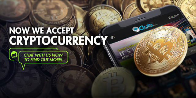
Crypto Deposit Bonus. This is another welcome bonus that is only available when depositing digital coins like Online, Online Cash, Ethereum, Litecoin and Ripple. The package includes gifts for the first five deposits totaling up to 0,24 BTC. This bonus cannot be used in live games. They give 30 days to wager.
VIP Reload. The operator promises a 50% bonus up to 0,013 BTC if the player replenishes the balance with at least 0,0027 BTC with the promo code. This is a weekly promotion available on Sundays only. The bonus amount and the deposit must be wagered 20 times in 7 days. Hump Day Special. Weekly reload allows you to get up to 0,0067 BTC to your deposit. The amount of the bonus depends on the amount deposited.
The bonus is available once a week on Wednesdays. The wagering requirements must be met within 7 days, after which the gift is canceled. Slots Stampede. 10 free spins weekly bonus offer. To use it, you need to scroll with rates over 0,013 BTC from Monday to Wednesday. The issued free spins are allowed to be used on Friday or Saturday.
Refer A Friend. No deposit bonus available to all users. For each attracted client, the player receives up to 0,0054 BTC. A beginner must make a deposit of at least 0,00067 BTC, and the user who invited him receives 200% of this amount.
Software and slot machines
The collection of games includes 300 titles, including about 180 slot machines. Gambling entertainment is represented by several developers: Betsoft, Nucleus Gaming, Fresh Deck Studios, Endorphina. Customers cannot play slot machines for free even after registration. When opening a page with video slots, users see two main blocks – with the most recently added and most popular titles. There are no filters for sorting machines, there is only a search by name.
Live dealer games at 9Club
Live casinos are divided into two categories. The Black section opens the gaming lobby of the provider Fresh Deck Studios. At the time of this writing, the page is not loading due to technical issues. The technical support promised to correct the situation soon. When you try to enter the second section with live games called Red, a notification about scheduled maintenance appears.
Other Crypto casino products
The operator decided to separate blackjack, table games and video poker by creating corresponding categories for them in the main menu. As with slot machines, there are no demos in these titles.
Tournaments. Casino founders allow their customers to win money by participating in many competitions. The operator paid special attention to blackjack tournaments. At the time of writing this review, two championships for this popular crypto casino card game are available on the site. Temporary tournaments are also held periodically. The operator allows you to follow the updates on the corresponding page.
Check in 9Club Casino
To start playing at 9Club online Casino on the official website, you need to register and top up your balance. Until this moment, it will not be possible to start any machine. The account opening procedure takes a little time.
A small form with the following fields appears in front of the visitor who opens the registration window with the following fields: name, surname, e-mail, password, country, postal code, phone number, date of birth. It is necessary to enter only reliable information in accordance with the passport data, so that in the future you will not encounter problems when verifying your account.
Mobile version of 9Club Casino
Almost all gambling games offered by the operator are available on mobile devices. An adapted version of the site has been developed for smartphones and tablets, which has received a somewhat simplified interface with hidden elements. The main menu does not clutter up the page but appears only by pressing the corresponding button. It is not possible to download the 9Club online Casino client or smartphone app separately.
Support
Anyone can contact technical support by e-mail, and online chat becomes available to players only after registration and entering the official website.
The competence of technical support specialists in the live chat is not at the highest level, therefore, if you have any non-standard questions, it is better to contact the administration immediately by e-mail.
Pros and cons
The 9Club casino is owned by the little-known operator, which operates under a Curacao license, but this information is not published on the site. A generous welcome offer encourages newbies to sign up, but one of them is considered a disadvantage of not being able to play slots for free at 9Club online Casino.
Best pros:
- the operator has a license
- welcome bonus up to 0,13 BTC
- gifts for inviting new players
- regular tournaments